
最新的Linux内核补丁确认,下一代AMD Zen架构将有12个CCD小芯片的整合封装。
目前的k10temp Linux温度监控驱动,只能支持最多8个CCD,每个8核心,最多64核心,而新驱动已经支持到12个CCD,对应产品家族为AMD Family 19h Models 10h-1Fh、A0h-AFh。
这显然针对的就是AMD Zen4。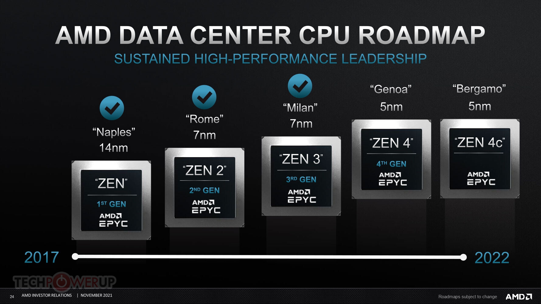
AMD Zen4 96核心准备就绪!Linux已支持12个CCD小芯片
事实上,AMD此前已经大方地公布,Zen4架构的霄龙处理器代号“Genoa”(热那亚),2022年量产上市,5nm工艺制造,支持DDR5、PCIe 5.0,最多96核心。
自然,每个CCD还是8核心。
据爆料,DDR5内存是十二通道,标准频率5200MHz,PCIe 5.0则是单路128条、双路160条,功耗320-400W。
Zen4还有个衍生版Zen4c,针对云服务优化,霄龙处理器代号“Bergamo”(贝尔格蒙),也是5nm工艺,最多128个核心。
如果每个CCD还是8核心,那就需要堆砌16个CCD。
另外据说,Zen4还会衍生出Zen4D,将会以大小核的方式搭配Zen5,2023年推出。
AMD Zen4 96核心准备就绪!Linux已支持12个CCD小芯片The latest Linux kernel patch confirms that the next generation AMD Zen architecture will have an integrated package of 12 CCD chiplets.
The current k10temp Linux temperature monitoring driver can only support a maximum of 8 CCDs, each with 8 cores and a maximum of 64 cores. The new driver already supports 12 CCDs. The corresponding product family is AMD Family 19h Models 10h-1Fh, A0h-AFh .
This is clearly aimed at AMD Zen4.
The core is ready! Linux already supports 12 small CCD chips. In fact, AMD has previously announced generously that the Zen4 architecture's Xiaolong processor code-named "Genoa" (Genoa) will be mass-produced and listed in 2022. It is manufactured on a 5nm process and supports DDR5 and PCIe 5.0. 96 cores.
Naturally, each CCD is still 8 cores.
According to the news, DDR5 memory has twelve channels, the standard frequency is 5200MHz, PCIe 5.0 has 128 single-channel, 160 dual-channel, and the power consumption is 320-400W.
Zen4 also has a derivative version of Zen4c, optimized for cloud services, the Xiaolong processor codenamed "Bergamo" (Bergamo), is also a 5nm process, up to 128 cores.
If each CCD is still 8 cores, then 16 CCDs need to be stacked.
In addition, it is said that Zen4 will also derive Zen4D, which will be used with Zen5 in the form of large and small cores, and will be launched in 2023.
The core is ready! Linux has supported 12 small CCD chips/generation Cores, which are commonly known as the "small and large core" hybrid architecture for the first time in the mainstream x86 field. According to the exposure, AMD Zen5 and Zen4D will also be combined.
According to the latest statement of the hardware exposure expert @Greymon55, the AMD Zen5 architecture desktop Ruilong product code-named "Granite Ridge" adopts 3nm and 6nm processes, of which 3nm naturally corresponds to the CCD computing part, and 6nm corresponds to the IOD input and output part. Small chip design.
The Ryzen product of the hybrid architecture is "Strix Point", which uses 3nm and 5nm processes.
This is a bit confusing. It seems that 3nm corresponds to Zen5 and 5nm corresponds to Zen4D. What about the IOD part? Continue the 6nm process? Then there are three processes at the same time.
As for the newly announced Zen4c architecture, @Greymon55 stated that it is different from Zen4D. Zen4c is cloud-oriented, Zen4D is not yet sure what it represents, it may be dense.
+Zen4D mixes three kinds of craft of big and small nuclear? 3nm+5nm+6nm According to previous news, Zen4D will completely redesign the cache system on the basis of Zen4 (three buffers may be less than half), streamline some features, reduce frequency and power consumption, the final result is to sacrifice a part of single-threaded performance in exchange for better Multi-threaded performance, and supports AVX512 instruction set, DDR5 memory, the core area is similar to Zen4.
It corresponds to the server Xiaolong product code-named "Bergamo" (Bergamo, a city in northern Italy). Each small chip integrates 16 cores, which is twice as large as the current one. The overall maximum is 128 cores. It is expected to be released in the second quarter of 2023.
Zen5 claims to be comparable to the increase in Zen and Zen2. IPC co-frequency performance is expected to increase by as much as 20-40% compared to Zen4. The birth time is expected in the fourth quarter of 2023.
The current plan for the hybrid architecture product of the two is to include 8 Zen5 large cores, 16 Zen4D small cores, a total of 24 cores, and 48 threads if they support multi-threading.
/
Intel Alder Lake 12代酷睿在x86主流领域首发俗称“大小核的”混合架构,而根据曝料,AMD Zen5、Zen4D也会组合在一起。
根据硬件曝料高手@Greymon55的最新说法,AMD Zen5架构的桌面锐龙产品代号“Granite Ridge”,采用3nm、6nm两种工艺,其中3nm自然对应CCD计算部分,6nm则对应IOD输入输出部分,还是小芯片设计。
Zen5+Zen4D混合架构的锐龙产品则是“Strix Point”,采用3nm、5nm两种工艺。
这就有点迷惑了,看起来应该是3nm对应Zen5、5nm对应Zen4D,那么IOD部分呢?继续6nm工艺?那就同时有三种工艺了。
至于新近公布的Zen4c架构,@Greymon55表示它和Zen4D是两回事。Zen4c是面向云服务的(cloud),Zen4D则还不确定具体代表什么,可能是dense。
AMD Zen5+Zen4D大小核混合三种工艺?3nm+5nm+6nm
根据此前消息,Zen4D会在Zen4的基础上,完全重新设计缓存系统(三缓可能少一半),精简一部分功能特性,降低频率和功耗,最终结果是牺牲一部分单线程性能,而换取更好的多线程性能,并支持AVX512指令集、DDR5内存,核心面积则与Zen4差不多。
它对应的服务器霄龙产品代号“Bergamo”(意大利北部城市贝加莫),每个小芯片内集成16个核心,比现在多一倍,整体最多128核心,预计2023年第二季度发布。
Zen5号称可以类比Zen、Zen2之间的提升幅度,IPC同频性能相比于Zen4有望提升多达20-40%,诞生时间预计在2023年第四季度。
二者的混合架构产品目前规划是包含8个Zen5大核心、16个Zen4D小核心,总计24核心,如果都支持多线程的话那就是48线程。